
Press Releases
"Isotropic shrinkage of patterned vacancies enables 3D nanoprecise metastructures for visible light applications"
株式会社フジクラ(代表取締役社長CEO:岡田直樹)は、米国マサチューセッツ工科大学(以下:MIT)のMechanical Engineering、Biological Engineering、および、McGovern Instituteに所属する研究者と「三次元ナノ加工技術」に関する共同研究を進めており、この度、共著で論文を発表し、科学誌NatureシリーズのNature Photonicsに掲載されました。
フジクラでは、2019年に新設したAdvanced Research Core(以下ARC)が先端基礎研究を行っており、複数のMITの研究室と連携しながらナノサイエンスおよびナノエンジニアリング分野における最先端の研究を推進しています。
Highlights of Research Achievements in 3D Nanofabrication Technology
One nanometer (nm) is one millionth of a millimeter, and three-dimensional nanofabrication technology refers to techniques for forming nanoscale structures and shapes with a high degree of freedom in three dimensions. Among nanometer-scale fabrication methods, lithography—widely used in the production of semiconductors and integrated circuits—is a representative approach. However, such methods are specialized in forming planar structures and therefore offer limited design freedom for creating complex three-dimensional structures.
The newly reported method, ImpCarv*1, is a photofabrication technique that constructs complex three-dimensional structures by scanning and exposing light in motion. It achieves a resolution far beyond the conventional “diffraction limit of light,” which has long been considered a fundamental challenge for photofabrication methods.
Photofabrication: Potential and Future Applications in Next-Generation Technologies
The photofabrication method, in which structures are formed by scanning and exposing light in motion, has the unique advantage of enabling the free fabrication of multiple structures even within a small plastic substrate of about 1 mm².
This makes it possible to create complex functional devices in which numerous functional elements are fabricated within a single substrate. Since these elements can be fabricated simultaneously, there is no need to precisely align and position them one by one, thereby improving production efficiency.
Moreover, the nanoscale microstructures produced by this method excel at precisely controlling various physical phenomena that occur at the nanoscale, making the technology broadly applicable across many fields. In particular, in the field of photonics, the ability to finely and flexibly control the shape, intensity, and phase of light opens the door to innovative photonic devices and components for optical communications and beyond.
In this study, a demonstration of an optical neural network*2 fabricated using the unique features of ImpCarv was also conducted. In a proof-of-concept experiment*3 using the four digits “1, 5, 6, and 7,” it was demonstrated that the optical neural network could classify numbers in a manner similar to artificial intelligence (AI).
This optical neural network is expected to have applications not only in optical communications, but also in optical computing—where light, rather than electrons, is used to perform high-speed calculations—and in next-generation robotics.
Fujikura will continue to promote research in the field of nano-innovation, contributing to both customer value creation and the resolution of social challenges.
【論文情報】
論文名:Isotropic shrinkage of photopatterned vacancies enables nanoprecise 3D
metastructures for visible-light optical computing
執筆者名: Quansan Yang1,2,3†, Gaojie Yang1†, Takahiro Nambara1,4, Hiroyuki Kusaka2,4, Yuichiro Kunai1,4, Alex C. Matlock2, Corban Swain1, Brett Pryor1, Yannick Salamin5,6, Daniel Oran1, Hasindu Kariyawasam7, Ramith Hettiarachchi7, Dushan Wadduwage7,8,9,10, Marin Soljačić5,6, Peter T.C. So2,11*, Edward S. Boyden1,11,12,13,14,15,16*
著者所属:1 McGovern Institute for Brain Research, Massachusetts Institute of Technology (MIT), Cambridge, MA 02139, USA.
2 Department of Mechanical Engineering, MIT, Cambridge, MA 02139, USA.
3 Department of Materials Science and Engineering, University of Washington, Seattle, WA 98195, USA.
4 Fujikura Ltd., Tokyo, 135-8512, Japan.
5 Department of Physics, MIT, Cambridge, MA 02139, USA.
6 Research Laboratory of Electronics, MIT, Cambridge, Massachusetts 02139, USA.
7 Center for Advanced Imaging, Harvard University, Cambridge, MA 02138, USA.
8 Department of Computer Science, Old Dominion University, Norfolk, VA 23529, USA.
9 School of Data Science, Old Dominion University, Norfolk, VA 23529, USA.
10 Department of Physics, Old Dominion University, Norfolk, VA 23529, USA.
11 Department of Biological Engineering, MIT, Cambridge, MA 02139, USA.
12 Department of Brain and Cognitive Sciences, MIT, Cambridge, MA 02139, USA.
13 Howard Hughes Medical Institute, MIT, Cambridge, MA 02139, USA.
14 K. Lisa Yang Center for Bionics, MIT, Cambridge, MA 02139, USA.
15 Center for Neurobiological Engineering, MIT, Cambridge, MA 02139, USA.
16 Koch Institute for Integrative Cancer Research, MIT, Cambridge, MA 02139, USA.
†These authors contributed equally to this work.
責任著者* Email: edboyden@mit.edu (E.S.B.) and ptso@mit.edu (P.T.C.S.).
掲載誌:Nature Photonics
掲載日(現地時間):2026年5月12日
掲載URL:https://www.nature.com/articles/s41566-026-01896-1
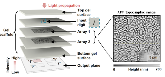
Schematic of an optical neural network demonstration (left) and results obtained by atomic force microscopy (right).
*1 ImpCarv
An acronym for Implosion Carving, a coined term that combines the meanings of “implosion” (contraction) and “carving.” It refers to a fabrication method in which a polymer is ablated and shaped by 3D scanning with a tightly focused light spot. In this approach, photofabrication is performed on a polymer in a swollen state, and the structure is subsequently contracted to yield the final form. This process enhances resolution and enables the creation of extremely small structures beyond the diffraction limit of light.
*2 Optical Newral Networks
A technology that performs computational processing simply by transmitting light through an optical circuit configured for computation. This approach enables high-speed processing while reducing power consumption.
*3 Proof-of-concept experiment
A process used to confirm the feasibility of a technology or idea, serving as a method to verify whether the underlying principle is valid.