
Vol. 05
The Superconducting Revolution
The story of the world's first "yttrium-based oxide superconducting wire" development

Phase 3
Development of superconductivity
Records are being broken one after another by improving deposition speed and critical current density, as well as by approaching longer lengths.
When the IBAD method was first discovered, its principle was verified using a small, stationary device. Due to the limitations of the device, the intermediate layer wire that could be produced here was only a few centimeters long. We then designed and built a device that could deposit the film while the initial substrate tape was moving. To demonstrate to the world that it would function as a wire, we considered the selection and placement of the ion source so that we could produce meter-class wire. We commissioned a heavy electrical equipment manufacturer with expertise in ion implantation technology to build the device, but they initially refused due to budget constraints. However, we were eventually able to get them to build it for a very low price, as they were willing to pay us for our promotion. Thus, the device was completed at the end of fiscal year 1992. Because this device required a long time for alignment, the wire production speed was only 10 cm per hour. As a result, it took several days of continuous day and night work to produce an intermediate layer wire of several meters.
After further improvements, the equipment was developed to be capable of producing 1m per hour. Eventually, it became possible to produce an intermediate layer 100m long. Furthermore, in the Y-based wire development project that began in 2003, the ion source was enlarged four times from 60cm x 8cm to 110cm x 15cm, so that a 500m-long intermediate layer could be produced at 5m/h. With this equipment, a superconducting wire 504m long and with an average critical current of 440A was realized at the end of 2007.
Furthermore, in order to improve the deposition speed, we are researching and developing intermediate layer materials and ion irradiation methods, and we will soon be able to achieve deposition speeds of several tens of m/h to 100 m/h.
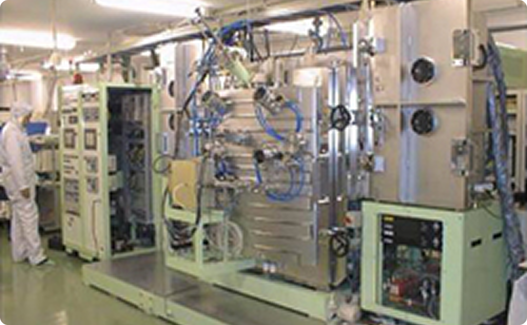
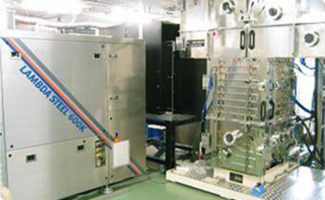
Development of "Large-size winding IBAD device"
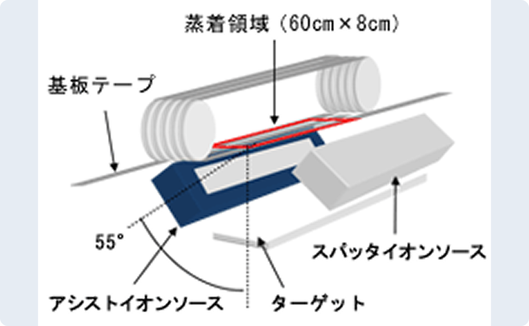
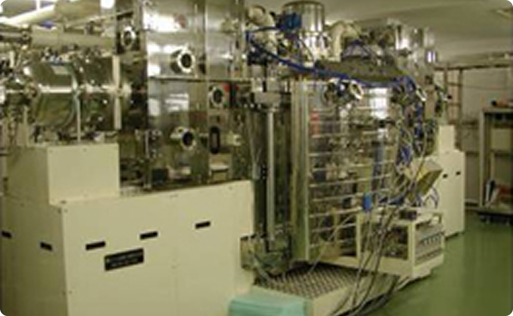
500m class IBAD deposition equipment
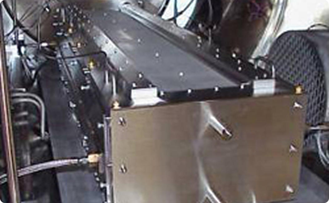
1.1m x 0.15m ion source
The properties of superconducting layers can be best realized by vapor deposition. Currently, the main vapor deposition processes are pulsed laser deposition (PLD), chemical vapor deposition (CVD), and metal-organic deposition (MOD). PLD involves irradiating a disk (called a target) made of sintered superconductor powder with a laser, resulting in particles being deposited on a substrate. This allows for high-speed deposition and low raw material costs, as the target can be directly made from primary materials such as yttrium oxide. By selecting temperatures of 800–900°C, appropriate oxygen gas, and laser irradiation conditions, superconducting wires with critical currents of several hundred amperes can be fabricated. Too low a deposition temperature results in the growth of a-axis particles, which do not contribute to superconducting current, while too high a temperature results in the decomposition of the deposited superconductor. Both methods result in low-critical-current films. To address this issue, efforts have been made to increase the output of lasers and improve temperature control methods, and while the critical current density was around 500,000 A/cm2 in the mid-1990s, it became possible to obtain long lengths of wire with a critical current density of over 1 million A/cm2 by around 2005. This was further improved to 2 million A/cm2 in 2007, and currently wires with a current density of over 3 million A/cm2 can be obtained.
-
 Vol. 01Mariana Trench RomanceThe story of cable development for the 10,000m-class unmanned exploration vehicle "KAIKO"
 -
 Vol. 02No.1 share in the worldThe story of the development of the de facto standard "Optical Fiber fusion splicer"
 -
 Vol. 03A gift from GodThe story of the development of "ultra-low loss Optical Fiber" a symbol of Fujikrism
 -
 Vol. 04Technology MicrocosmThe development story of "Flexible Printed Circuits (FPC)," the key to the evolution of electronic devices
 -
 Vol. 05The Superconducting RevolutionThe story of the world's first "yttrium-based oxide superconducting wire" development
Management Philosophy


- HOME
- Company Information
- Fujikura History
- FUJIKURA ODYSSEY
- Vol.05 Superconductivity Revolution