Research and Development
New Research & Development Activities for the Future
|
Kenji Nishide |
|
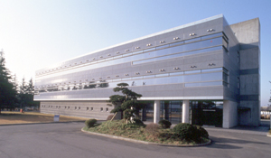
Introduction of a laboratory: Advanced Technology Laboratory
|
|
|
Major research fields
Photonics
|
|
|
Energy
|
|
|
Electronics
|
|
|
New Products and Technologies
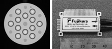
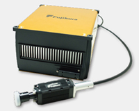
■Development of High-power Pulse Fiber Laser FLP-G75S
|
|
FLP-G75S |
■Fujikura Honored by the Laser Society of Japan with Laser Industry Award for Excellent Products
Fujikura was honored by the society with "laser industry award 2015 for excellent products" for our fiber laser product line including 4kW continuous wave fiber laser.
|
|
|
|
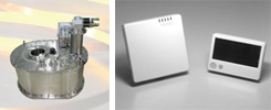
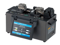
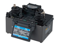
■Start of Sales of Large-core Fiber Cleavers and Fiber Recoaters
Fujikura is pleased to announce the development and the start of sales of large-core fiber cleavers (CT-105, CT-106) and fiber recoaters (FSR-05, FSR-06, FSR-07), tools for use in the assembly of equipment at plants and research and development.
▼Large-core Fiber Cleaver (CT-105, CT-106)
A large-core optical fiber refers to a quartz-based fiber with a cladding diameter larger than that of a common telecommunications fiber. Large-core fibers are used in industries such as those of lasers and other devices, where transmission of high-power light energy is needed, and sensors.
We have developed two models of large-core fiber cleavers capable of cutting a fiber with a maximum clad diameter of 1,250 μm and launched the sales.
Since the products have a system for automatically adjusting forces to hold optical fibers, they are also suitable for cleaving photonic crystal fibers and capillaries (hollow glass tubes). The CT-106 is capable of cleaving diagonally.
▼Fiber Recoaters (FSR-05, FSR-06, FSR-07)
A method to protect a spliced section of an optical fiber is coating the stripped glass with UV-cured resin. This method can keep a spliced section thinner and lighter than the method using a reinforcement sleeve.
We have developed and started marketing of three models of fiber recoaters that offer users options regarding the strength checking system of a spliced section according to use. These products achieved greater accuracy in finished shape, longer life of consumable products, and higher maintainability than previous models.
|
CT-106 |
FSR-07 |
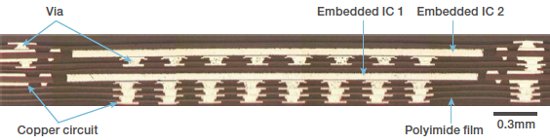
■Development of Chip-stack WABE PackageTM
Fujikura has developed Chip-stack WABE PackageTM (wafer and board level device embedded package), a circuit board into which several IC chips are embedded vertically, and put it into use for the first time in the world.
Chip-stack WABE PackageTM uses technologies of WABE PackageTM, which has components built in polyimide multi-layer circuits and is currently in mass production. The method of stacking IC chips allowed dramatic downsizing of the electronic circuit. Through the use of polyimide films as the base material, the board with two-stack IC chips achieved a thickness of as small as 0.4mm.
Chip-stack WABE PackageTM is the world's-first technology to meet the needs in industries, where smaller and thinner electronic circuits are strongly demanded, such as those of wearable electronics and medical / healthcare devices. We will supply the most suitable solution to our customers in these advancing industries.
|
Cross-sectional view of Chip-stack WABE PackageTM |